
Events
Events
Subject: Top-down Fabrication into Sub-nanometre Scale in Low-dimensional Systems
Time: 14:30, May 28, 2014
Address: Takada Hall, School of ME
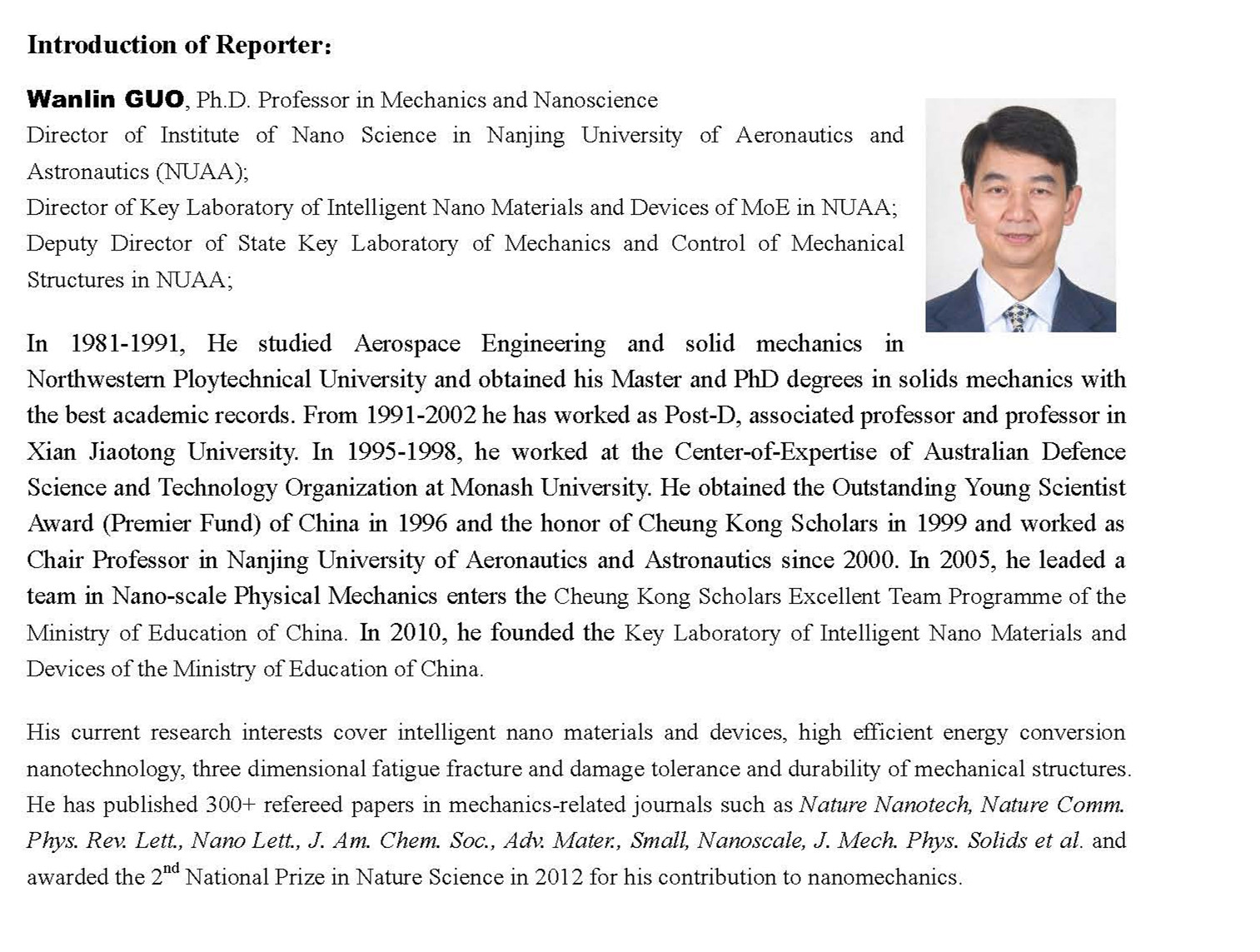
Reporter: Prof. Wanlin Guo
Abstract:
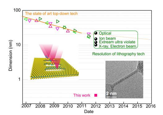
To fabricate functional devices with smaller feature structures in controllable way is always the driven force for our modern industry. The development in industry technologies is propelling the dimension of devices down to 10-nanometers, but facing great challenges in manufacture at sub-10-nanometer scale. Nanotechnology can fabricate nanoribbons from two-dimensional atomic crystals such as graphene well ranged into sub-10-nanometers, but their geometries and properties become hard to control1. Here we analyze the recent breakthrough of top-down technology for fabrication of molybdenum-sulfide ribbons with uniform sub-nanometer width simply by electron irradiation from mechanically exfoliated molybdenum disulfide (MoS2) layer2. This work opened a window to a novel top-down route for controllable fabrication of sub-nanometre building blocks for functional devices, proposing an effective strategy to avoid the limitation of lithography resolution. An important novel conception revealed here is that spontaneous phase transition of the irradiated material at sub-nanometre scale is essential for the breakthrough, showing the importance of intrinsic coupling between top-down and bottom-up process. Similar process for creating sub-nanometre wires in other two-dimensional materials will be predicted in this report and new evidences will be introduced.
Two-dimensional materials themselves can be obtained through either top-down or bottom-up methodology3, and can bring the exceptional properties at one atomic layer thickness into our macro-world, promising plenty of rooms for technology revolution. For example, we recently found that drawing a droplet over monolayer graphene can induce electric potential, the so called drawing potential4, waving seawater across graphene can generate more electricity5. These novel electrokinetic phenomena are found to be unique to graphene like nanofilms, open route for novel functional devices and energy harvesting6.
I would also like to share our understanding and experience in the past tens years about graphene related low-dimensional materials, such as h-BN, MoS2 and other new 2D materials will be introduced with our theoretical and experimental experiences being share, the concurrent challenges in nanotechnology being discussed.
The triangles and solid circles stand for the reported dimension of flash 1/2 pitch6 and lithography resolutions, respectively. The solid and dot lines are the time lines of flash industry (//www.itrs.net/). Lift insets, fabrication of sub-nanometre wires by driving holes in two-dimensional transition metal dichalcogenides. Right inset, a resulted sub-nanometre wire2.
Reference
1. Novoselov, K. S. et al. A roadmap for graphene. Nature 490, 192-200 (2012).
2. Liu, X., Sun, L. T. & Guo, W. et al. Top-down fabrication of sub-nanometre semiconducting nanoribbons derived from molybdenum disulfide sheets, Nature Commun. 4, 1776, (2013).
3. Li, X., Yin, J., Zhou, J., & Guo, W. (2014). Large area hexagonal boron nitride monolayer as efficient atomically thick insulating coating against friction and oxidation. Nanotech. 25, 105701. (2013).
4. Yin, J., Li, X., Yu, J., Zhang, Z., Zhou, J. & Guo, W. Generating electricity by moving a droplet of ionic liquid along graphene. Nature nanotechnology 9 (5), 378-383 (2014 May).
5. Yin J. & Guo, W. et al. Waving potential in graphene. Nature communications 5, 3582 (2014 May 6).
6. //nanotechweb.org/cws/article/tech/57149 .

Shanghai Jiao Tong University
Address: 800 Dongchuan Road, Shanghai
200240